Complex Oxides at Argonne
Oxide MBE at Argonne National Laboratory, Center for Nanoscale Materials (CNM)
The Electronic & Magnetic Materials & Devices group of CNM uses DCA R450 oxide MBE system to grow complex oxides. Dr. Anand Bhattacharya’s research focuses on correlated states that emerge in complex oxides at interfaces, in ordered analogs, and due to nanoscale confinement.
This custom design oxide MBE system is an excellent example of DCA’s custom design capabilities. The system was designed and manufactured based on Dr. Bhattacharya’s design.
Dr. Bhattacharya explores new ways to realize and manipulate collective states in the complex oxides. The oxide layers are grown in atomic layer-by-layer manner using ozone as the oxidizing gas. The technique allows the growth of heterostructures and superlattices with atomically sharp interfaces between constituent materials. A variety of tools is used to probe the states that arise in these structures, including transport and magnetic measurements, scattering with neutrons and x-rays, and scanning probes.
The recent list of publications is here: Argonne publication list
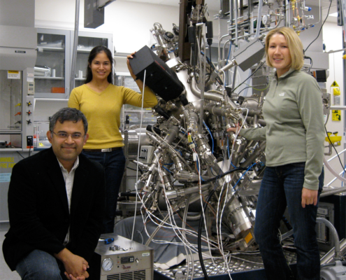
Argonne researchers Anand Bhattacharya, Tiffany Santos, and Brittany Nelson-Cheeseman with Argonne’s Center for Nanoscale Materials custom complex oxide molecular beam epitaxy instrument. Photo courtesy of ANL.
Oxide MBE at the Materials Physics Laboratory of the University of Texas at Austin
Prof. Alex Demkov’s group at the Material Physics Lab is currently pursuing several key areas of epitaxial oxides including integration of complex oxides with semiconductors, controlling the interface between dissimilar materials using Zintl phases, all-oxide quantum wells and superlattices, strain tuning of electronic properties, oxidation and growth mechanisms of oxides on semiconductors and wetting of metals on oxide surfaces.
The M600 MBE system is the core facility of the Materials Physics Laboratory. The multi-chamber UHV systems has a linear UHV sample transfer line which connects the MBE chamber with a home-build ALD system, an XPS/UPS system and a home-build STM. The M600 is equipped with six effusion cells (four standard and two high-temperature), a four-pocket electron beam evaporator, an rf plasma atomic nitrogen source, and an rf plasma atomic oxygen source with high-precision piezoelectric leak valve.
Recent publications by Prof. Demkov’s group: Recent Publications by Materials Physics Lab
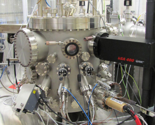
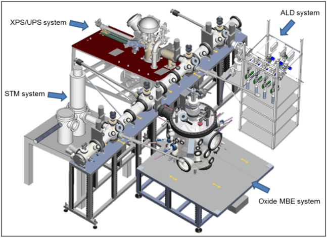
M600 oxide MBE system. Photos courtesy of the Materials Physics Laboratory at the University of Texas in Austin.
200 mm Oxide MBE System at the Leibnitz University of Hannover
Prof. Hans-Jörg Osten’s research group at Institute of Electronics Materials and Devices of the Leibnitz University of Hannover, Germany, uses DCA S1000 multi-chamber MBE system for their oxide growth. The MBE system has maximum substrate size of 200 mm and includes UHV metallization, XPS analysis and high temperature pre-cleaning facilities. The wafer handling is fully automatic and based on a UHV cluster tool.
They recently reported of the growth of strained Si1-xGex layers on Si substrates following the growth of epitaxial Gd2O3 thin films on Si1-xGex. Pt/Gd2O3/Si1-xGex/Si stacks were fabricated by several in situ process steps. In situ processing was possible due to the multi-chamber design of Prof. Osten’s MBE system. The structural and electrical characterization revealed excellent interface properties for Gd2O3/Si0.8Ge0.2 on both Si(111) and Si(001) substrates. They concluded “Si1-xGex with its superior electron and hole mobility together with epitaxial high-K dielectrics could provide the solution for semiconductor industries to further continue the Moore’s law in the future”.
List of publications by the Institute of Electronic Materials and Devices
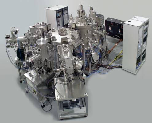
S1000 oxide MBE cluster tool with 200 mm wafer size.
Oxide MBE at the Shanghai Institute of Microsystem and Information Technology (SIMIT)
Dr. Dawei Shen at the Shanghai Institute of Microsystem and Information Technology (SIMIT) has recently setup a state-of-the-art growth and analysis facility for complex oxide growth and characterisation.
At heart of the facility is a DCA R450 MBE system which is combined with an Angle-Resolved Photoemission Spectroscopy (ARPES) chamber allowing sample transfer under UHV between the two. The system is installed at the Shanghai Synchrotron Radiation Facility. The system is used to study interfacial superconductivity, electronic structure of SrRuO3 films and topological superconductor candidates such as CrO2/TiO2 and VO2/TiO2.
Recent publications:
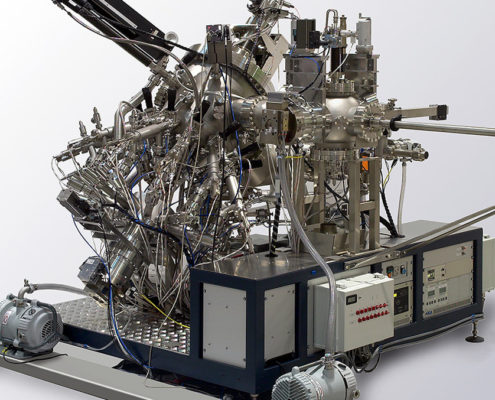
R450 oxide MBE system at SIMIT. Photo courtesy of Dawei Shen, SIMIT.
Dual R450 Oxide MBE System at the Max Planck Institute for Solid State Research
The Scientific Service Group Technology at the Max Planck Institute for Solid State Research develops advanced epitaxial growth technologies to deposit complex compounds with atomic-layer precision. Dr. Gennady Logvenov’s group uses pulsed laser deposition (PLD) and oxide MBE to synthesize thin films, multilayers and superlattices of different complex oxides including cuprates, manganates, nickelates, cobaltates, ruthenates.
The group has a new unique dual chamber R450 Oxide MBE cluster tool system, consisting of two UHV growth chambers and one central distribution chamber (CDC) with automatic wafer handling.
The cassette load lock chamber allows a quick loading of the substrate into the growth chamber, and the storage chamber allows the storage of the substrate under UHV conditions. Each growth chamber is equipped with 10 differentially pumped effusion cells and one multi-pocket electron gun.
An ozone delivery system is integrated in the MBE is used for the oxygenation during the process. Electro-pneumatic linear shutters provide an accurate control of the layer-by-layer deposition process with a precision of a small fraction of an atomic monolayer.
The modular design of the MBE system allows an easy and fast reload or replacement of each metal source. This provides a great flexibility in depositing different complex oxides compounds including high temperature superconductors.
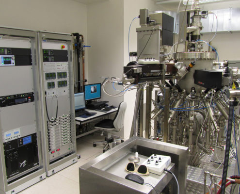
View of one of the R450 growth chambers. © Max-Planck-Institute for Solid-State-Research
