Nanowire Growth at the Laboratory of Semiconductor Materials, EPFL
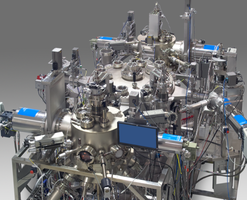
Prof. Anna Fontcuberta i Morral’s group uses a dual chamber P600 MBE system to investigate novel semiconductor nanostructure combinations using mainly nanowires. Semiconductor nanowires represent a unique system for exploring phenomena at the nanoscale and are also expected to play a critical role in future electronic and optoelectronic devices and biochemical sensors.
The DCA MBE system at EPFL features fully automatic substrate transfer system with a UHV cluster tool, hydrogen pre-clean chamber, high temperature outgassing stage and a UHV storage chamber. Both growth chambers are equipped with solid sources for GaAs growth.


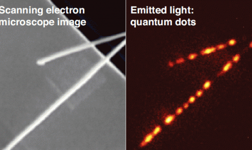
Prof. Fontcuberta i Morral’s group has discovered a new way of emitting photons one at a time. They have constructed semiconductor nanowires with “quantum dots” of unprecedented quality – a discovery with implications for the future of quantum computing. Photo courtesy of EPFL.
GaN Nanowire Growth at the Paul-Drude-Institut für Festkörperelektronik
The goal of our research is to inspire and demonstrate new functionalities for optoelectronic applications by employing III-V nanowires. To this end, we investigate fundamental nanowire properties that crucially influence such applications and in particular light-emitting diodes. We grow both group-III-nitride and group-III-arsenide nanowires by molecular beam epitaxy, typically on silicon substrates and without any external catalyst. We analyze their microstructure and their optical as well as electronic properties, and we employ technology to guide growth, enable electrical measurements, and process demonstrator devices.

SEM images illustrating the morphology of the samples when the growth is interrupted at the three different stages depicted in figure (a) corresponds to the incubation stage, (b) to the nucleation stage, and (c) to the elongation stage. The insets show the corresponding RHEED patterns along the [112̅0] azimuth. Data and images courtesy of Paul Drude Institute.
